Clock signals are fundamental to the operation of nearly all modern electronic systems, including computers, servers, industrial controllers, and consumer electronics. These signals provide the precise timing required to synchronize digital circuits, allowing processors, memory modules, and peripherals to operate in a coordinated manner. However, the very characteristics that make clock signals fast and precise—rapid rise and fall times, high frequencies, and repeated periodic switching—also make them a major source of electromagnetic interference (EMI). These emissions, if not properly controlled, can degrade the performance of nearby electronics and violate regulatory electromagnetic compatibility (EMC) standards.
The emissions from clock signals arise primarily due to the high di/dt (rate of change of current) and dv/dt (rate of change of voltage) associated with digital transitions. Fast switching edges generate broad frequency spectra containing both harmonics of the fundamental clock frequency and high-frequency noise components. These signals can radiate from the clock traces themselves, from associated power supply lines, or from connectors and cables attached to the device. The energy is often coupled into nearby circuitry via capacitive and inductive coupling, producing unintended currents and voltages that may disrupt sensitive analog or digital systems.
PCB layout and component placement play a critical role in mitigating emissions from clock signals. Traces carrying clock signals must be routed with minimal length and over continuous ground planes to reduce loop area, which is directly related to radiated emissions. Designers often implement differential clock lines, which carry equal and opposite currents; this arrangement causes the radiated fields to partially cancel, significantly reducing emissions. In addition, clock traces may be shielded or routed internally within multilayer boards to further limit radiation.
The power supply network is another pathway for clock-induced emissions. Switching currents from high-speed clocks can couple into power and ground planes, generating voltage fluctuations that propagate through the system. To counteract this, engineers incorporate decoupling capacitors close to clock drivers and oscillators. These capacitors act as local energy reservoirs, reducing high-frequency current spikes and stabilizing voltage rails. Proper selection of capacitor values, placement, and low-impedance paths to ground is critical for minimizing conducted emissions.
Signal integrity considerations are also intertwined with EMC performance. Uncontrolled reflections, ringing, and overshoot on clock traces can create additional high-frequency components that increase emissions. Techniques such as controlled-impedance traces, proper termination, series damping resistors, and edge-rate control are used to suppress these effects. Slowing down the rise and fall times of clock edges can dramatically reduce the spectral energy in higher-frequency bands without significantly affecting overall system performance.
Another advanced method to reduce emissions is spread-spectrum clocking. By slightly modulating the clock frequency over time, the energy that would normally concentrate at discrete harmonics is spread over a wider spectrum, lowering peak emissions. This technique is particularly effective for systems that must meet stringent regulatory limits, such as CISPR 32, FCC Part 15, or EN 55032. Spread-spectrum clocks must be designed carefully, however, to avoid timing errors or phase mismatches in synchronous circuits.
High-frequency clocks can also interact with nearby passive components, including inductors, traces, and connector pins, potentially creating resonances that amplify emissions at certain frequencies. Proper layout, filtering, and grounding strategies are required to suppress these resonances. In some cases, EMI filters, ferrite beads, and shielding enclosures are applied around the clock circuitry or cables to prevent radiated emissions from escaping the equipment.
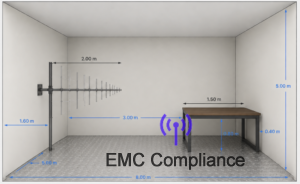
Finally, EMC compliance requires systematic testing of clock-generated emissions. Both radiated and conducted emissions are measured using specialized setups, such as anechoic chambers and line impedance stabilization networks (LISNs). Test results often inform iterative design improvements, including modifying trace layouts, adding damping networks, and optimizing decoupling strategies. Because clock signals are one of the dominant sources of EMI in most electronic systems, careful design and testing are critical for both product reliability and regulatory approval.
In conclusion, while clock signals are indispensable for digital electronics, they are inherently high-risk sources of electromagnetic emissions. Effective mitigation requires a combination of oscillator selection, trace routing, grounding, differential signaling, decoupling, edge-rate control, spread-spectrum techniques, and shielding. By understanding the mechanisms by which clock signals generate EMI and applying these mitigation strategies, engineers can ensure that electronic equipment operates reliably while meeting strict EMC standards.
Mitigating Clock Emissions and Harmonics in Electronics
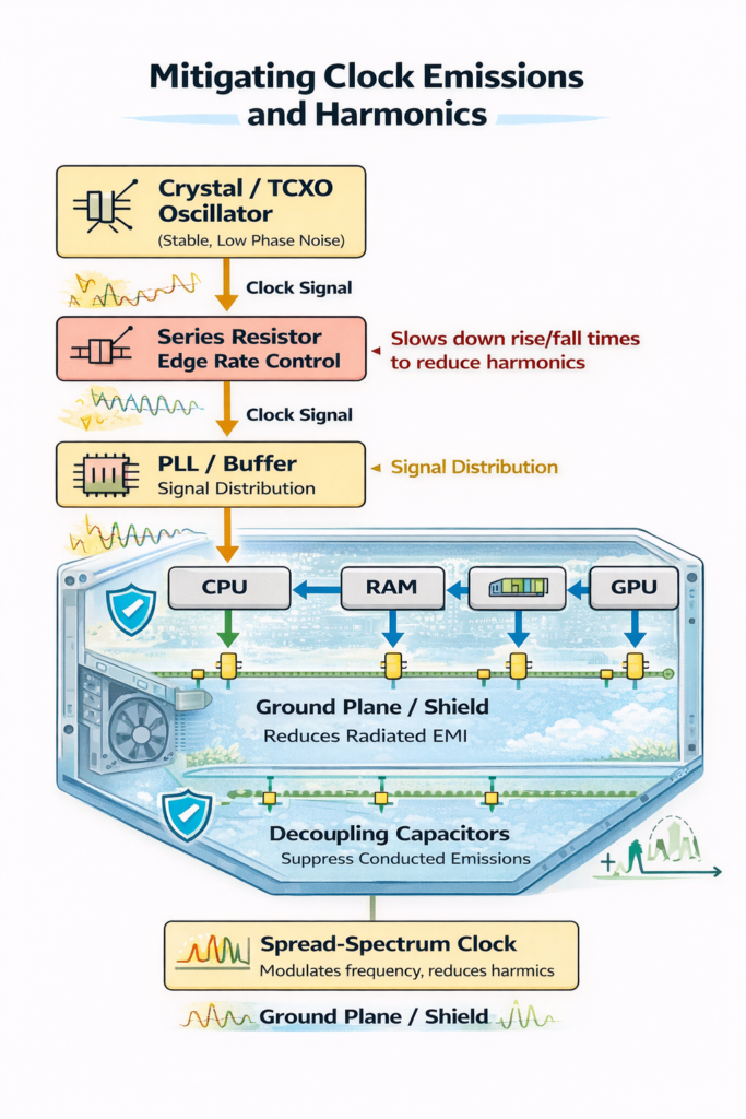
Clock signals, by their nature, are one of the primary sources of electromagnetic interference (EMI) in electronic equipment. High-frequency edges generate a broad spectrum of harmonics, which can radiate from traces, cables, and connectors. These harmonics can interfere with nearby circuits and violate EMC standards. Fixing clock emissions requires a combination of circuit design, PCB layout, signal integrity, and filtering techniques.
One of the first approaches to mitigate clock harmonics is edge-rate control. Rapid rising and falling edges produce strong high-frequency spectral components. By adding small series resistors or RC damping networks at the output of clock drivers, the slew rate of the signal can be slowed slightly, reducing high-frequency harmonics while preserving timing accuracy. Designers must carefully balance edge-rate reduction with system performance requirements, as too slow edges can cause timing errors in high-speed digital circuits.
PCB layout and trace design are also crucial. Clock traces should be short, direct, and routed over continuous ground planes to minimize loop area, which is directly proportional to radiated emissions. Differential clock signaling is highly effective, as equal and opposite currents in the differential pair naturally cancel radiated fields. In addition, controlled impedance routing prevents reflections and ringing, which can introduce additional high-frequency harmonics. Avoiding stubs and carefully terminating clock lines are essential for maintaining signal integrity and reducing EMI.
Another effective mitigation strategy is spread-spectrum clocking. By slightly modulating the clock frequency, the energy that would normally concentrate at discrete harmonic frequencies is spread over a wider spectrum, reducing peak emissions. This technique is widely used in computers, servers, and consumer electronics to pass regulatory limits like CISPR 32 and FCC Part 15. However, spread-spectrum must be applied carefully to avoid introducing phase jitter that could disrupt synchronous circuits.
Power supply decoupling and filtering are also important. High-speed clock currents can induce voltage fluctuations on power and ground planes, creating conducted emissions. Placing high-frequency decoupling capacitors near clock drivers and oscillators reduces these voltage spikes. Ferrite beads and LC filters can be added to clock supply lines or outputs to suppress unwanted harmonics without affecting the fundamental clock frequency.
Finally, shielding and enclosure design help contain any residual radiated emissions. Sensitive clock traces can be routed under copper pours or inside shielded areas of the PCB. EMI gaskets, grounded shields, and metal enclosures prevent emissions from escaping the system while also protecting the clock from external interference. Testing under both radiated and conducted EMC standards is essential to validate that mitigation strategies are effective.
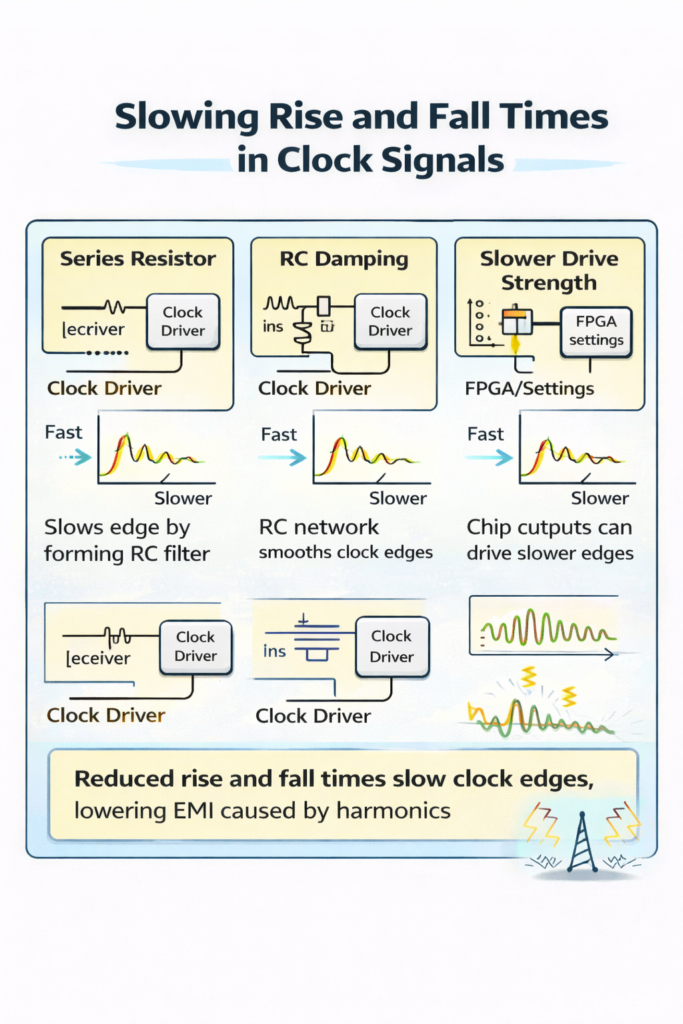
Slowing Rise and Fall Times in Clock Signals
Clock signals in digital electronics have sharp transitions from low to high (rising edge) and high to low (falling edge). While fast edges are desirable for timing precision, they generate high-frequency harmonics that can cause electromagnetic interference (EMI) and signal integrity problems. Slowing the rise and fall times, also called edge-rate control, reduces the high-frequency spectral content of the signal, mitigating radiated and conducted emissions. The key is to carefully manage the trade-off between slower edges and system performance, as too slow transitions can cause timing errors or logic misinterpretation.
One of the simplest methods to slow edges is to insert series resistors in the clock path. By adding a small resistor (often tens of ohms) in series with the output of a clock driver or buffer, the resistor combines with the parasitic capacitance of the trace and input pins to form an RC low-pass filter. This filter smooths the voltage transitions, reducing the rate of change of the signal. The value of the series resistor must be carefully selected: too small and it has little effect; too large and it can degrade voltage levels or timing margins. Designers often simulate the RC effect using SPICE or signal integrity tools to choose an optimal value.
Another approach is to use slower drive-strength settings available in many modern FPGAs, microcontrollers, or clock driver ICs. These devices often provide programmable output drive currents; reducing the drive strength inherently slows the transitions without requiring additional external components. This technique is convenient because it doesn’t consume board space and can be tuned dynamically in some systems. Care must be taken to ensure that slower edges still meet setup and hold timing requirements for all downstream components.
For high-speed circuits, controlled impedance traces combined with damping networks can also help slow edges. Small RC networks or ferrite beads placed close to the driver output act as frequency-dependent attenuators, suppressing the fastest components of the clock waveform. Designers must consider PCB trace capacitance, parasitic inductance, and the input capacitance of receiving devices, because these factors determine the effectiveness of edge-rate control and overall signal integrity.
Finally, simulation and measurement are essential. Edge-rate control should be verified using oscilloscopes with sufficient bandwidth to observe the transitions and ensure that rise/fall times are within the target range. It’s also common to measure EMI emissions in an EMC test environment to confirm that the mitigation techniques effectively reduce harmonic content. Balancing slower edges for EMI reduction with reliable digital operation is a core part of high-speed PCB design.