Digital clocks are fundamental to almost all modern electronic systems. They provide the timing reference that synchronizes operations in microcontrollers, processors, communication interfaces, and digital logic. While essential, clock signals are also one of the primary sources of electromagnetic interference (EMI), making them a key concern in EMC design.
Clock Signals and Switching Edges
A digital clock is typically a periodic square wave alternating between logic high and low states. Although it may appear simple, the critical feature from an EMC perspective is the switching edge—the rapid transition between these states.
These edges are not truly instantaneous, but in high-speed circuits they can be extremely fast (nanoseconds or less). Fast rise and fall times mean the signal contains a wide range of high-frequency components (harmonics), not just the fundamental clock frequency. For example, a 50 MHz clock can generate significant energy well into the hundreds of MHz or even GHz range.
These high-frequency components are what make clock signals strong sources of radiated and conducted emissions.
Impact on EMC
Fast switching edges can negatively affect EMC performance in several ways:
- Radiated Emissions:
Clock traces on a PCB can act like antennas. The faster the edge, the more high-frequency energy is available to radiate into free space. - Conducted Emissions:
Clock signals can couple into power and ground planes, spreading noise throughout the system and potentially onto external cables. - Crosstalk:
High dV/dt (rate of voltage change) can capacitively couple into adjacent traces, while high dI/dt (current change) can induce noise through mutual inductance. - Ground Bounce and Switching Noise:
Simultaneous switching of digital signals can cause fluctuations in the ground reference, leading to unintended emissions and signal integrity issues.
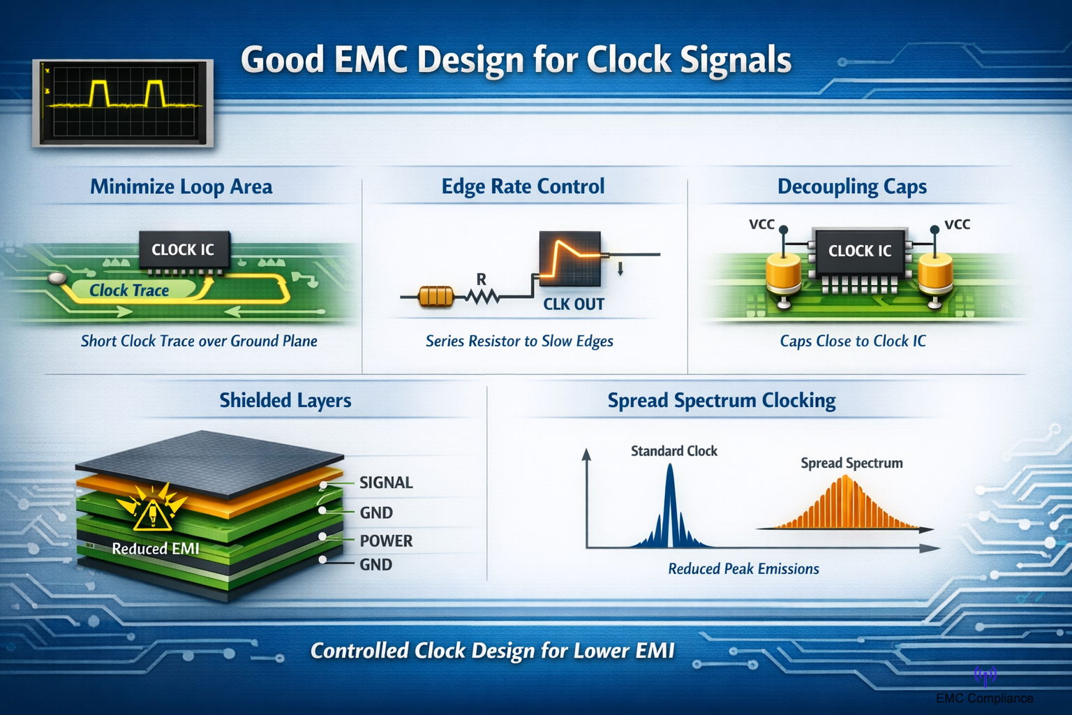
Design Considerations for EMC
To reduce EMC issues related to digital clocks, designers must carefully control how clock signals are implemented:
- Minimize Loop Area:
Keep clock traces short and route them over continuous ground planes to reduce radiation. - Controlled Impedance Routing:
Proper impedance matching reduces reflections and ringing, which can worsen emissions. - Edge Rate Control:
Slowing down rise and fall times (where possible) reduces high-frequency harmonics. This can be done using series resistors or selecting devices with controlled slew rates. - Proper Decoupling:
Place decoupling capacitors close to clock-generating ICs to suppress high-frequency noise on power rails. - Shielding and Layer Stack-up:
Use ground planes and appropriate PCB layer arrangements to contain electromagnetic fields. - Clock Distribution:
Avoid unnecessarily routing clocks across large areas of the PCB. Use buffering and localized distribution where needed. - Spread Spectrum Clocking (SSC):
Slightly modulating the clock frequency spreads energy over a wider band, reducing peak emissions.
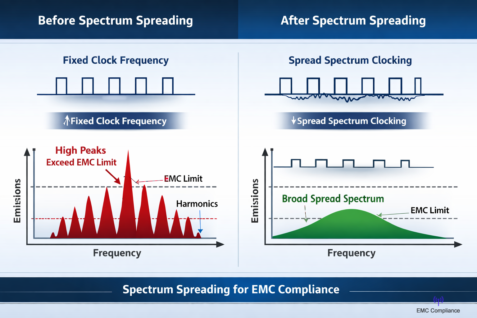
Spectrum Spreading of a Clock in Electronic Circuits (EMC Perspective)
In digital circuits, clock signals are one of the main sources of electromagnetic emissions because they are periodic and contain sharp switching edges. A standard clock operates at a fixed frequency, meaning most of its energy is concentrated at that frequency and its harmonics. This creates narrow, high peaks in the frequency spectrum, which are more likely to exceed EMC limits and cause interference with other systems.
Spectrum spreading, often referred to as spread spectrum clocking (SSC), is a technique used to reduce these peak emissions. Instead of keeping the clock frequency constant, the clock is deliberately varied slightly over time. This variation is usually very small (typically less than ±0.5% of the nominal frequency) and is often done using a low-frequency modulation signal.
How Spectrum Spreading Works
Rather than producing a single sharp frequency spike, the clock energy is distributed over a wider range of frequencies. In other words, the same total energy is present, but it is “spread out” across a band instead of being concentrated at one point.
This results in:
- Lower peak amplitude at any single frequency
- Reduced likelihood of failing EMC radiated or conducted emission tests
- Less interference with nearby sensitive circuits or communication systems
The modulation used is often triangular or sinusoidal, and it continuously sweeps the clock frequency up and down around its Centre value.
EMC Benefits
From an EMC standpoint, the key advantage is peak reduction. Regulatory standards typically measure the maximum emission at specific frequencies. By spreading the energy, the measured peak at any one frequency drops, even though the total emitted energy remains similar.
This can make a significant difference in passing compliance tests, especially for high-speed digital systems where clock harmonics extend into sensitive RF ranges.
Design Considerations
While spectrum spreading is useful, it must be applied carefully:
- Timing Sensitivity:
Some circuits (e.g. high-speed serial links or precise timing systems) may not tolerate frequency variation. - Modulation Depth and Rate:
Too much variation can cause system instability, while too little may not provide enough EMC benefit. - System Compatibility:
All parts of the system must be able to operate correctly across the slightly varying clock frequency. - Not a Substitute for Good Layout:
Spread spectrum helps reduce emissions, but it should be used alongside proper PCB design practices such as good grounding, short clock traces, and controlled impedance routing.